
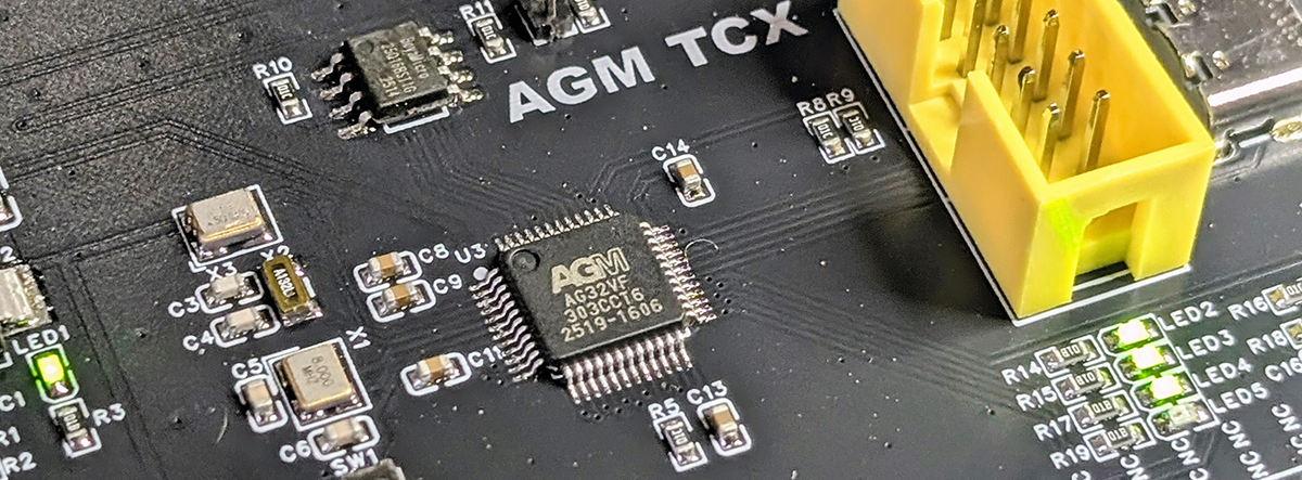
AGaMEMnon: An Open Source Toolchain for a $1 RISC-V Chip With an FPGA Bolted On
An open-source synthesis, place-and-route, and bitstream flow for the AGM AG32 / AGRV2K embedded FPGA fabric with no proprietary vendor executable
The AG32 from AGM Micro is a combination microcontroller and FPGA. It’s a real RV32IMAFC core with hard peripherals, plus a small programmable fabric sitting between those peripherals and the pins:
- RV32IMAFC core @ 248 MHz, hardware FPU
- 256 KB Flash (zero-wait), 128 KB SRAM
- 5× UART · 2× I²C · SPI
- 1× CAN 2.0 · USB FS+OTG · Ethernet MAC
- 3× 12-bit ADC (17 ch, 3 MSPS) · 2× 10-bit DAC
- 2× comparator · RTC · watchdog
- basic + advanced timers
- 2112 LUT4s
- 2112 flip-flops
- 4 block RAMs
- 1 PLL
- 4 global clocks
- up to 128 I/O (74 for the 100 pin package)
This FPGA fabric is the configurable glue that attaches almost any pin to any peripheral. You can route a UART to almost any pin, drop a state machine into a signal path, add a custom peripheral next to the CPU, and have it all configure from SPI flash at boot. That makes the AG32 unusually good for flexible pin assignment, protocol glue, deterministic IO, and small custom hardware without a separate FPGA. Think of this chip as something like the Cypress PSoC, but it’s better because it’s an actual FPGA bolted to a RISC-V core.
This is an STM32-class chip, but RISC-V, and an FPGA, in one package. Pinmuxes just happen. Do you like the PIOs on the RP2040? Cool, here's something better. It costs a dollar.
The AG32 has hardly any English-language documentation. The only thing I know about it comes from LLM-translated PDFs. The standard way to create bitstreams for the FPGA is through a Windows-only installation of a clone of Altera Quartus II. The only way to get this software is off a Baidu Netdisk link, with the password 12ej. Your only option for generating bitstreams for the FPGA is a black box: AGM’s af.exe fabric back-end. Can you read Chinese? Fuck you if you want to use this chip the way the manufacturer intended.
Project AGaMEMnon takes Verilog and produces a flashable AG32 fabric bitstream — synthesis, pack, place, route, and bitstream generation — with no proprietary vendor binary anywhere in the path. The RISC-V side already had GCC. This is the IceStorm for a chip no one has heard about.
The Chip In Question
First an overview of the AG32, which I am uniquely qualified to talk about because all the documentation is in Chinese, and I spent the tokens to translate them. These are the best block diagrams you’re going to get:
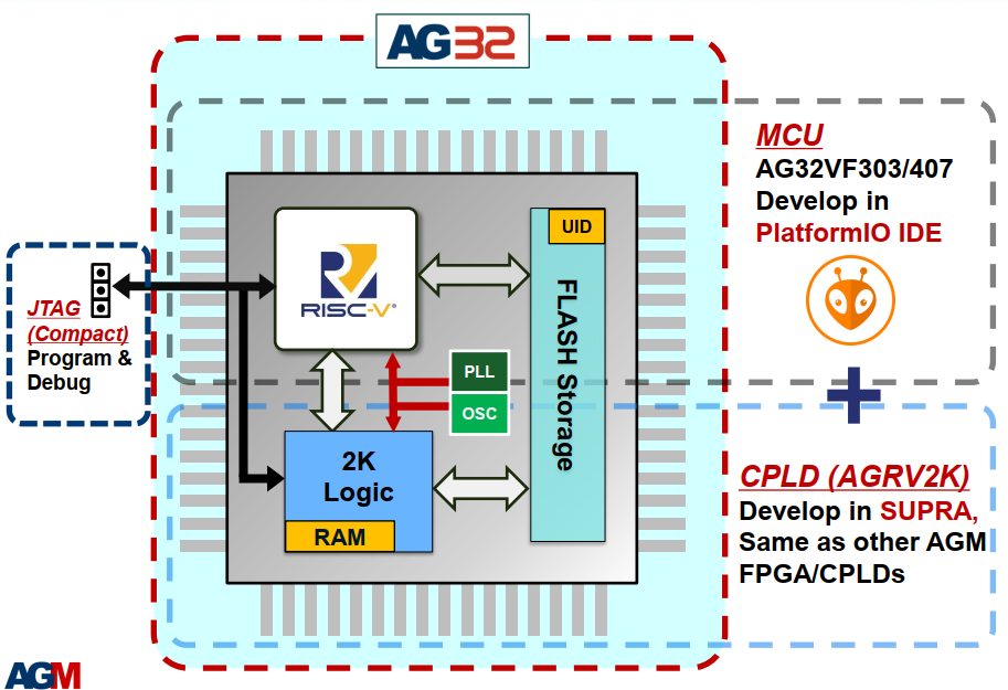
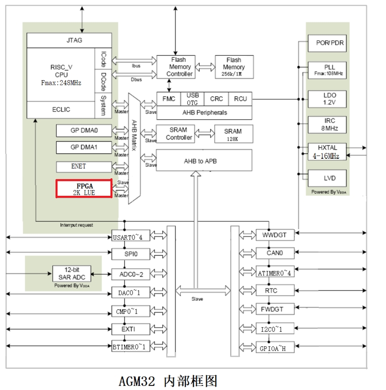
Half of this is normal. The microcontroller part of this chip is a RISC-V core, specifically a RV32IMAFC and supported by GCC. Up to 1MB of Flash is supported, and 128k of SRAM is available. The chip has a maximum clock frequency of 248MHz, and has five UARTs, two I2Cs, and USB, CAN, and SPI peripherals. There’s ADCs. There’s timers. The product numbers for these parts range from AG32VF103 to AG32VF303 to AG32VF407, telling you these are heavily inspired by the STM32 line of microcontrollers. Some of these chips have an on-die 8MB PSRAM. These chips cost about a dollar or two. LCSC has some in stock.
The other half of this chip is weird. It’s a 2K LUT FPGA stuck in between the pins and the peripherals of the RISC-V core. On a normal microcontroller, the UART is mapped to specific pins. The AG32 doesn’t have fixed mapping at all. All of the RISC-V peripherals are dumped into the FPGA fabric, and the FPGA decides where they go. This isn’t a crossbar, because you can put logic in there too. You can put a state machine behind a peripheral, and do deterministic I/O without interrupts. It’s like the Cypress PSoC, except the fabric is a real LUT-based FPGA.
As far as the FPGA goes, the fabric, or at least how it’s programmed, is an Altera clone. You’re supposed to program it with a fork of Quartus II. The logic cells are named alta_slice and the placements are LCCELL_X1001_Y1001. At power-on a block called the Flash Config Block reads an LZW-compressed bitstream out of the SPI flash, and shifts it into the fabric before the CPU is allowed out of reset. This is heavily inspired by an Altera FPGA from 2003, with a RISC-V core sitting next to it, sold for a dollar.
This would be an awesome chip if any of this were documented in English, or if it had any modern tooling at all.
Reverse Engineering The Chip
The ‘normal’ way to reverse engineer an FPGA, if there is one, is painful. Claire Wolf did this more than a decade ago with Lattice iCE40 parts. This reverse engineering task was done with statistical analyses of working bitstreams. This was hard. But this was done years ago, and on a toolchain that wasn’t a carbon copy of what Altera was doing twenty years ago.
The AG32 is heavily derived from the Altera MAX II / Cyclone family of parts, chips programmed with Quartus II, given the migration table in some of the AGM manuals (EPM240 → AG256, EP4CE10 → AG10K). The AG32 toolchain is the Kirkland branded version of the toolchain for old Altera parts, from the clone of the Altera USB-Blaster, to ‘Cyclone IV’ being found in the derived architecture files, to the use of Quartus project files, to the “Megafunction/IP” model. This is Quartus II, reimplemented on pin-compatible, but not identical, silicon.
This similarity gives us a few different but familiar-looking layers to the AG32 toolchain. First, Supra.exe, the GUI IDE, does all the project management, compiling, generating, and timing tuning. This is just a GUI, with all the actual work being done by af.exe. This is the engine that has an embedded Tcl interpreter, an embedded copy of yosys, the architecture database, and all pack, place, route, bitgen, and flash-file generation happening in one Windows executable.
From there, af.exe generates the fabric bitstream and the JTAG programming file. The important thing is that af.exe has an interpreter that handles commands from the GUI, and does literally everything for generating bitstreams for the AG32 FPGA.
The iCE40 project was released in 2015 after person-years of work inspecting the Lattice chips from the outside. But Ghidra was released in 2019, and af.exe gives me a window into how the AG32 chips are programmed. You can see where I’m going with this. Just throw af.exe into Ghidra, and I’ll be able to learn something about this chip.
Just Throw Ghidra At The Problem
 So yeah, just throw Ghidra at the problem.
 af.exe is a 12.4 MB MinGW/GCC program, and stripped it’s 12 megabytes of unlabeled soup. But, af.exe has a scripting layer, and every Tcl command registers itself with an argument-spec string like oo:alta::decode_file_from_to. The Java…. script walks through all the command-name strings, finds the implementing function, and decompiles it.
Pulling the usable data out of af.exe completely relied on this decompilation. The arch database looked encrypted, but was actually a substitution cypher. I found this out after pulling these lookup tables, reimplementing the constructor in Python, then checking if encode(decode(x)) == x. It worked, and the same cypher ended up decoding the routing files too. It was the same for every bit of this project, from proving the CRC algorithm for the configuration engine, to figuring out the logic map. Build something with the reverse engineered toolchain, build the same thing with the real toolchain, and count the diffs. That’s how I proved the CRC (it’s CRC-32/BZIP2, checked by the config engine before it’ll accept a bitstream), the LZW codec, and the logic map. I found the routing graph for the MCU / IO / BRAM / clock boundary as route.AGRV2K.bar.gz sitting right there in the install directory.
However, simply decompiling af.exe isn’t sufficient. The easiest way to pull out everything out of af.exe is to decompile and debug, setting watchpoints in code and whatnot. However, af.exe has a double-dereferenced “license check” that was really hard to track down. Without passing this license check, I couldn’t run the program, and watchpoints wouldn’t fire. It turned out the license check was looking for a license file. The content of this file in the stock toolchain was, THIS IS A TRIAL KEY FROM ALTA. That’s it. That’s the entire license system for af.exe.
Like bro. I mean technically that’s security.
Now The Fuckin Thing Doesn’t Work
At this point I had the format, whatever ‘encryption’ counts for, the logic and memory map. What I didn’t have was the RRG, the routing resource graph for the LUTs. This is the map for every wire in the FPGA, which wires connect to what, and the config bits that selects each one. The RRG doesn’t exist as a file. It only exists as an algorithm as an algorithm in af.exe.
Instead of disassembling that and trying to figure out what it did, I did the stupid thing that works and generated a bunch of Verilog and scattered them across different tiles so the router inside af.exe is forced onto different wires each time. You can script this. At the end you have a bunch of .csv files which contains the full routing graph.
Topologically, this worked. I could route a wire on a graph, af.exe would route it, but when I put it on silicon, nothing came out the other end. It was like this with everything; links to BRAM would be inexplicably dead, clock signals wouldn’t send the clock to other parts of the chip.
Which wires physically conduct is not stored anywhere. It’s not in the arch files, it’s not in route.bar, it’s not a table I could dump. It lives only inside the router’s cost model, computed fresh, per-design, at route time, and thrown away. I spent a genuinely stupid amount of effort trying to catch it — reading the RRG out of memory after a route, breakpointing the edge-builder and dumping every candidate it considered, chasing pointers that turned out to be stack locals torn down on return. The geometry was all there and correct. The identity, “this specific wire, at this specific tile”, was not.
So I Made The Chip Reverse-Engineer Itself
At this point, I had access to the RISC-V half of the chip. I could talk to some of the FPGA. I could have those two communicate, somewhat. I could even blink GPIO pins. The only way to get a complete RRG is to ask the chip about itself. I’d generate a tiny bit of Verilog that forces a signal down one specific wire in the fabric. Put it in the SRAM and read the far end of this path, either through the RISC-V core, reading a register the wire lands on, or by wiring up a Pi Pico as an improvised logic analyzer on the GPIO pins.
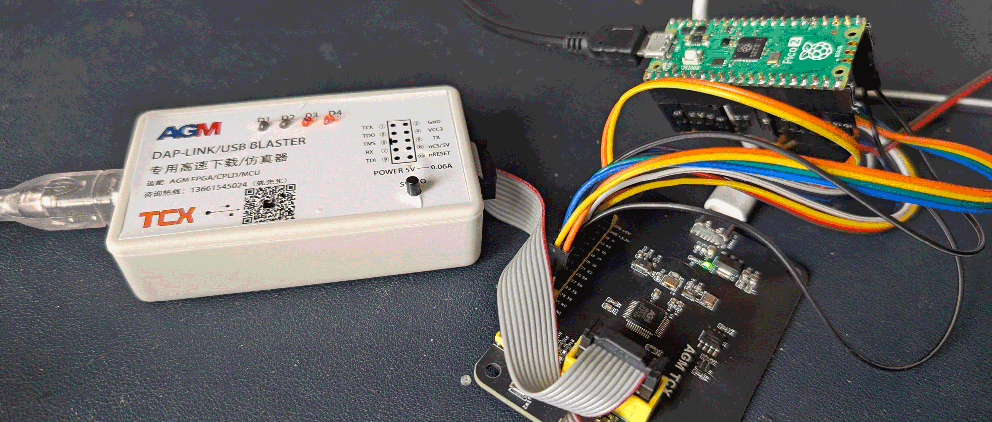
So, write the Verilog and read the other end. If it toggles, the wire conducts. If it doesn’t, it’s a dead link in the RRG. Do this tens of thousands of times. This is a great job for an LLM, by the way. Just give it a CSV of candidate wires in the FPGA fabric, and it will write the Verilog and the RISC-V firmware to test each one, inject it into the SRAM of the chip, drive the board, read the results, and update the map. The result is a device model that is an actual measurement. And with a complete map of what every wire, every bel, every pip, and what every LUT in the FPGA does, we have an open toolchain.
So Now We Have An Open Toolchain
Bolt yosys on the front, give nextpnr the measured device model, and it’s the whole pipeline: synthesis, pack, place, route, bitstream, flasher. Shove Verilog in, get a bitstream out, flash it over a cheap CMSIS-DAP probe, and the fabric does what you told it to on real silicon — combinational logic, flip-flops, counters, state machines, clocking across the array, driving real pins, and the CPU reading and writing it over the bus. No af.exe, no Quartus, no Windows, no Baidu, no vendor binary anywhere in the path.
All of this can be inspected by comparing the Verilog with what is produced with af.exe, same placement in, nearly the same bits out, and verified. The placer and router don’t always pick the same wires af.exe would because place and route is non-deterministic, but the bitstream they produce is valid and works.
To be honest, this isn’t a big lift; AGM built a program with a scripting layer that told me everything I needed. I consider this an ‘I can use Ghidra’ project rather than an ‘I made an open toolchain for an FPGA’ project, but I see how those could be conflated.
Demo Time
The AG32 is a really interesting chip. It’s a RISC-V with a 2k LUT FPGA bolted to it. The smallest RISC-V softcore can comfortably fit inside that. There’s only one real project I can demo this with:

This demo exists, but I didn’t feel like filming it:
Actually Acquiring This Chip
This chip is unknown to most parts distributors. There is one source for a dev board: the official AGM Micro store on Taobao. This link is probably going to be dead at some time in the future, so here’s a screencap:
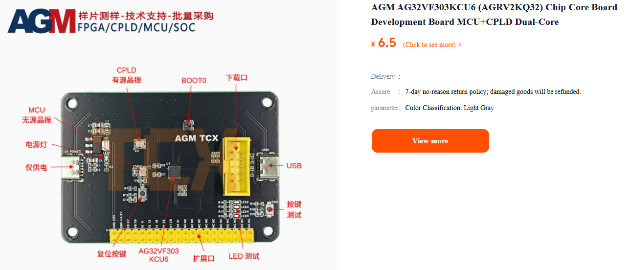
LCSC has a few chips in stock in various packages, although I’ve never seen them have more than 2000 of any one part at a time. This probably means they’re just getting single reels every once in a while.
That’s it. Those are the only places I can find this chip for sale. But with a toolchain that doesn’t suck, hopefully this chip will gain a little bit of popularity and AGM Micro will figure out better distribution channels. This hope is a little selfish on my part; I’m working on a project where I need thousands of these chips.
The Name.
It’s named this because I had ‘AG32’, ‘FPGA or CPLD’ and ‘Memory’ to work with. AGaMEMnon was fine. I want to go on record that this was named before Nolan’s Odyssey was released, even if it was published after. I am also mentally preparing for Marc Andreessen quoting Aeschylus when Trump finally dies.