
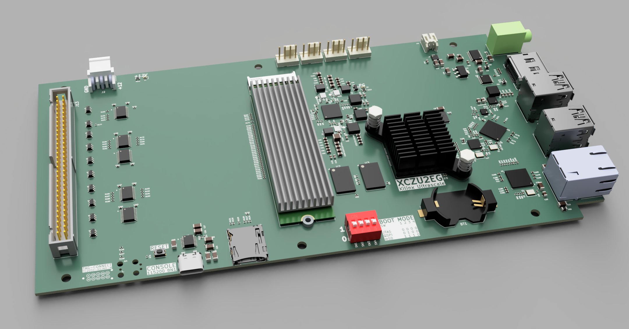
A Zynq UltraScale+ Single-Board Computer
For another project I needed a Linux with a lot of real-time I/O. A Raspberry Pi can’t do it, building my own computer with a Rockchip SoC won’t do it, and bolting an FPGA to a seperate Linux SoC is the wrong way to do it.
If you want hard real-time I/O with Linux, your options are limited. Microchip has a PolarFire SoC, Intel/Altera has the Cyclone V, the same chip in the MiSTer, and AMD/Xilinx hs the Zynq-7000, Ultrascale+, and the Versal family of chips. Those are all the reasonable options if you want a chip that’s an FPGA+Linux SoC. I went with the AMD/Xilinx Ultrascale+, a 784-ball BGA package that is theoretically in the same ballpark as a Raspberry Pi 3.
Specs
The top-line numbers for this board make it something like a 10-year-old Raspberry Pi, but that doesn’t tell the whole story. Here’s the specs:
| SoC | AMD/Xilinx Zynq UltraScale+ MPSoC — XCZU2CG-2SFVC784I |
| CPU | Dual-core Arm Cortex-A53 @ 1.5 GHz / Dual-core Arm Cortex-R5F real-time CPU |
| Memory | 4 GB DDR4-2400, 32-bit bus, ~9.6 GB/s |
| Storage | M.2 NVMe (PCIe Gen2 ×1, ~500 MB/s), microSD, QSPI boot flash |
| Networking | Gigabit Ethernet (hardened MAC + RGMII PHY) |
| USB | 4× USB 3.0, 5 Gbps |
| Display | DisplayPort 1.2, 2-lane — 4K @ 30 Hz or 1080p @ 60 Hz |
| Real-time fabric I/O | Banks of independent hardware UARTs and jitter-free timing, straight from the PL |
On paper, that’s a Raspberry Pi 3. In reality, the Pi3 has LPDDR2 that was slow as shit; mine has DDR4. The Pi3 has SD card storage, mine has NVMe. The Pi3 had USB 2, this board has USB 3.2 Gen 1x1 SuperSpeed 5Gbps, or whatever the hell the USB-IF is calling it. The Pi has 100 Mbps Ethernet hanging off a USB hub, I have 1 Gbps Ethernet. For the Ultrascale chips, the CPU is still limited to an ARM Cortex-A53, but the storage, memory, and I/O is at least comparable to a laptop. And this chip is bolted to an FPGA, which no other single board computer will ever have.
The Hardware
The main chip is the XCZU2EG-2SFVC784I, part of AMD/Xilinx Zynq UltraScale+ MPSoC family. The XCZU2EG is a Quad-core Arm Cortex-A53 chip. There’s a Mali-400 GPU on there, PCIe Gne1/2, DisplayPort 1.2a, USB 3.0, and enough peripherals to turn this into a real computer. There are dual Arm Cortex-R5F real-time cores. This is also an FPGA, and that part of the chip has about 100k logic cells, 5.3Mb of block RAM, and enough LUTs to do what I want to do.
The first spin of this board used a XCZU2CG, the dual-core version of the ~EG variant. Other than having only two Cortex-A53 cores and not having a Mali-400 GPU, this is the same chip as the harder to obtain ~EG variant. The JLCPCB order included the ~CG variant because it was available on LCSC, with the option of switching over to the ~EG variant once I can confirm the DDR trains and the peripherals work.
So now I have to turn this into a real computer:
Power
The XCZU2EG requires ten independent power rails:
| Net | Voltage | Net | Voltage |
|---|---|---|---|
+3V3 | 3.3 V | +1V2_VDDQ | 1.2 V |
+0V85_VCCINT | 0.85 V | +0V6_VTT | 0.6 V |
+1V2_MGTAVTT | 1.2 V | +2V5_VPP | 2.5 V |
+0V9_MGTAVCC | 0.9 V | +3V3_PSIO | 3.3 V |
+1V8 | 1.8 V | +1V8_MGTAVCCAUX | 1.8 V |
This is insane, but TI has an off-the-shelf part for Xilinx chips, the TPS6508640RSKT. Just follow the suggested layout in the application notes and you can get something that’ll work.
Ultimately, power is provided from a +12V MeanWell power supply.
Memory, Fast and Slow
The chip supports DDR4, so I’m using that. The SFVC784 package physically lacks the pins for a full 64-bit memory bus. By filling the available 32-bit bus with two 16Gb SK Hynix chips, the dual-core A53 has a 4GB memory pool. This is fine. It does what I need.
“Disk” storage is a bit better, with a single PCIe Gen2 x1 lane routed to an M.2 connector. This gives me NVMe storage, as much as I want. Bandwidth maxes out around 500 MB/s.
USB
The Zynq has one USB 3.0 controller but no built-in USB 2.0 PHY. Two external chips are required: a Microchip USB3300-EZK ULPI PHY for USB 2.0 signaling, and a TUSB8043A 4-port hub to fan out to four USB-A 3.0 ports on the rear panel. I can get 5Gbps out of one USB port, bandwidth shared across all ports. The +5V_USB rail is supplied by a dedicated TPS568215 buck converter capable of 8 A continuous output.
Ethernet
The Zynq Processing System includes four hardened Gigabit Ethernet MACs directly in the silicon, giving the Ubuntu kernel native, zero-overhead networking without burning CPU cycles on software drivers. Ethernet is provided by the Realtek RTL8211EG-VB-CG from RGMII pins on the Zynq.
DisplayPort
The Zynq Processing System’s hardened video controller outputs native DisplayPort. Rather than adding an expensive, hard-to-source active converter chip to translate to HDMI, I put a standard full-size DisplayPort receptacle (Foxconn 3VD51203-3D6A-7H) directly on the rear I/O panel. Two high-speed GTR lanes from Bank 505 drive the DisplayPort signal directly to the connector. If I need HDMI, I can use a standard $10 active DP-to-HDMI dongle.
The Buttload of SPI links
This is the reason I need an FPGA + Linux combo. I need to talk to 16 different boards simultaneously, in hard real time, with either serial or SPI communication (I haven’t decided which yet).
The UARTs live in the FPGA fabric as 16 independent hardware AXI UART Lite instances, each with its own AXI-Lite register window and its own IRQ line routed through the PL-to-PS interrupt fabric. All 16 UART channels are routed through the Zynq’s HD I/O banks. The High-Performance (HP) banks (64, 65, 66) are limited to 1.8V and are reserved for future expansion.
The 32 UART signals (16 TX + 16 RX) are split across two banks:
- Bank 25 carries Cards 0-7 (16 pins: 8 TX + 8 RX)
- Bank 26 carries Cards 8-15 (16 pins: 8 TX + 8 RX)
These signals, plus a few others, are routed through a 60-pin Harting shrouded IDC header on the edge of the board. 60-pin IDC connectors are much harder to find than their 50-pin sisters.
Hardware Reasoning
In short, this would have been an unbelievable single board computer in 2015. It’s 2026, though. The shortcomings – a single lane of PCIe 2.0 to the NVMe slot, DDR4 that is capped at half the bandwidth it could achieve if it was a 64-bit bus, and my post-hoc realization that I could have just put an SFP Ethernet module on this board – relegate it to something thats okay, but not the best at anything.
This is a bad single-board computer, but it’s also the only way to get 16 bidirectional serial links sitting on the same silicon as a Linux box. That’s the point. I needed Linux and an FPGA on a custom board with some weird features. This was the only way to do it.
Building It With JLCPCB
The choice of the SFVC784I package for the Zynq is not random – this is the only package for an UltraScale processor that uses a 0.8mm pitch BGA; all other packages are down in the 0.4mm to 0.6mm size range. I chose this so I can use the cheapest process available on JLCPCB. No blind and buried vias, and a standard, non-HDI 8-layer stackup. Here’s the layers, as a zoomable .SVG:
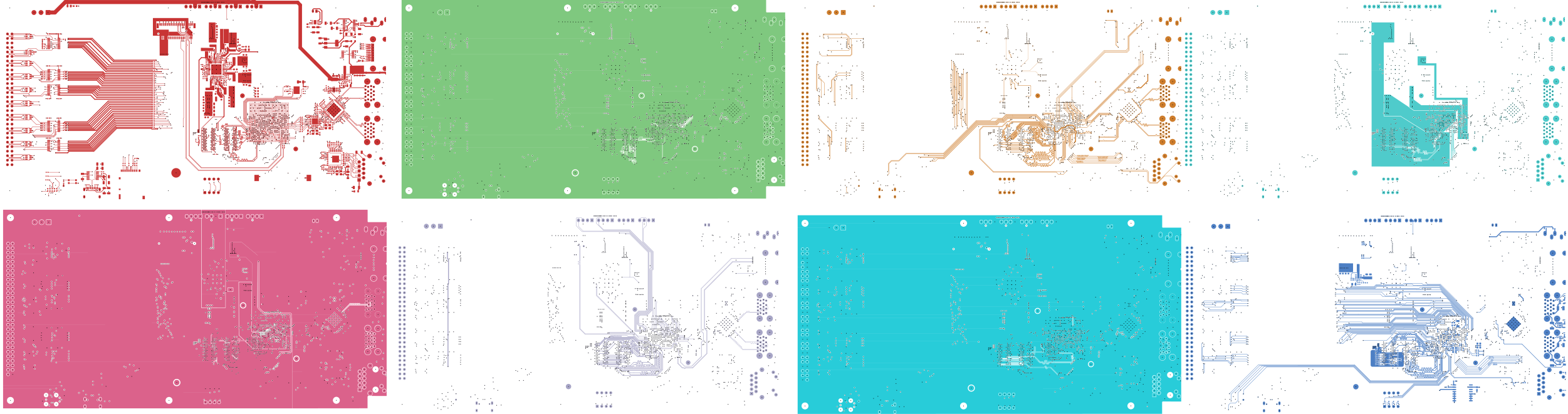
The full 8-layer stackup. Click to enlarge, then scroll to zoom into the layer labels.
This is fucking insane. I have a job. I make money. Why on Earth would I do DDR4 on the cheapest process JLCPCB has? Why wouldn’t I use a 12-layer PCB, as recommended in the Xilinx docs? Mostly because I could, and because I saw an UltraScale dev board that advertised itself as being an 8-layer board (for cost reduction). This is the most engineer-brained marketing I’ve ever seen, apart from any project made with Rust, so I had to try it myself.
About $2000
That’s the answer to your question. And that’s for two. About $1700 of that was for the standard 8-layer JLCPCB stackup, another $80 because I used 0.15 mm/0.25 mm vias. I also needed a few parts from Mouser (60-pin IDC connectors, ribbon cable, heatsinks, thermal interface sheet, and some hardware), putting the total cost for two boards at about $2000. This doesn’t include an M.2 NVMe drive, so there’s that, too.
One substitution of note, LCSC did not carry a differential LVDS oscillator when I ordered the boards. I also bought a Microchip DSC1123CI1-027.0000T from Mouser to service the 27MHz GTR reference clock. Six pins, and easily solderable with a hot air gun.
Board Bringup
<!–
AI-DRAFTED SCAFFOLD — summary of generated prose, NOT your words. Everything ABOVE “## The Hardware” is your own writing. Rewrite the sections below in your own voice, then delete this whole comment. ================================================================
THE HARDWARE
- Picking the silicon: XCZU2EG-2SFVC784I. EG family = dual A53 + dual R5F + Mali-400 GPU + programmable logic on one die; -2 speed grade -> 1.5 GHz @ 0.85 V. PRODUCTION HOOK: 784-ball BGA at 0.8 mm pitch routes on a standard 8-layer pooled-prototype board (no HDI, no microvias) -> “anyone can build it” vs. a specialty house + five-figure minimum.
- Memory: 4 GB DDR4-2400, 32-bit bus, fly-by, ~9.6 GB/s. Tradeoff: package lacks the pins for a 64-bit bus; chose routability over bandwidth (I/O-bound board).
- Transceiver budget (the central constraint): only 4 PS-GTR lanes -> 2 to DisplayPort (no HDMI converter IC), 1 to PCIe Gen2 x1 NVMe (~500 MB/s), 1 to USB 3.0. Clocking trap: PCIe wants 100 MHz, DP/USB want 27 MHz -> two LVDS oscillators.
- Real-time I/O in the fabric (the whole reason for the board): many independent hardware UARTs in PL, each its own register window + IRQ, kernel out of the hot path; PL also makes jitter-free timing/strobes Linux can’t. The half no SBC has.
- Networking / storage / boot: hardened GbE via RGMII PHY; 4-port USB 3.0 hub via ULPI; M.2 primary storage; triple boot (JTAG / QSPI / microSD) via DIP switch.
- Power & thermal: TPS6508640 PMIC, 7-rail tree, strict UG1085 sequencing; ~40 W typ / 50 W peak from 12 V; quad-fan PWM.
THE SOFTWARE
- Three-CPU AMP: Linux on the 2x A53 (acts like a workstation); the 2x R5F walled off for deterministic real-time + housekeeping, free of kernel preemption.
- Surviving a kernel panic: real-time work, on-board console, and management live on separate cores/power domains, so they survive a Linux panic; you only lose Linux-side stuff (new jobs, SSH, filesystem).
- BMC for free: baseboard management controller on the spare R5F core -> out-of-band console + a scrapable metrics endpoint; shares the single Ethernet MAC via a fabric screener so BMC + host present two MAC/IP addresses down one cable.
WHERE IT ENDS UP
- Net: a manufacturable Linux+FPGA SBC with workstation storage/networking, deterministic fabric I/O, and server-grade management. A reusable platform.